2019-计算机组织与结构-lecture07
Internal Memory
1. 回顾:存储器
- 存储器由一定数量的单元构成,每个单元可以被唯一标识,每个单元都有存储一个数值的能力。
- 地址:单元的唯一标识符(采用二进制)
- 地址空间:可唯一标识的单元总数
- 寻址能力:存储在每个单元中的信息的位数
- 大多数存储器是字节寻址的,而执行科学计算的计算机通常是64位寻址的,也就是264
- 字节可寻址(64b/32b)、字可寻址(8b)、按位寻址(1b)
- 寻址能力的影响因素:归根结底是因为设计时的地址的长度。
- 地址总线的根数
- 寻址机制的不同
- 计算机的内存真正能真正使用的内存大小的影响因素:
- 地址空间
- 寻址能力
- 最终是由上面两个之一来决定的。
- 例子:4G内存的电脑加上8G的内存条,不会变快,因为寻址能力不会变强,被制约。
- 地址空间越大,容量会越大吗?
- 不一定,每个单元(屋子)的大小不同。
1.1. 主存结构
- 主存存储器由多达2n个可寻址的字组成,每个字有一个n位的地址。
- 比如一个存储器是64M *16位的,那么就是16位的数据,64MB是地址数量。
- 一个字节(1 B = 8 b),(1KB = 210B = 213b)
2. Main memory
- 这一章主要是来讲在在内存金字塔中的cache下面的主存Main Memory部分。
2.1. Semiconductor Main Memory(半导体主存储器)
- The use of semiconductor chips for main memory is almost universal
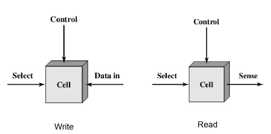
- Memory cell(存储位元): 是最基本的组成部分,basic element of semiconductor memory,
- Properties
- 呈现两种稳态:稳定或者半稳定的保持两个状态,分别代表0和1。They exhibit two stable (or semi-stable) states, which can be used to represent binaries 1 and 0
- 能够写入信息(至少一次)来设置状态。They are capable of being written into (at least once), to set the state
- 可以被读出状态信息。They are capable of being read to sense the state
2.1.1. Memory Cell Operation(存储器位元操作)
3. Semiconductor Memory Types(半导体存储器类型)
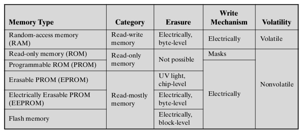
- 讲述的所有的存储器都是随机访问存储器
3.1. Read-write memory(读写存储器)
3.1.1. RAM(随机访问存储器)
- Random-Access Memory(随机访问存储器)
- Characteristics
- Reading/writing can be easy and rapid(可以被轻松地时常地写入写出)
- Volatile(易失性):一旦断电,存储的数据丢失。极其重要
- Types
- DRAM: Dynamic RAM(动态:动态是指一种存储电荷丢失的趋势)
- SRAM: Static RAM(静态)
- 这里面的单元是指寻址单元而不是Cell
- DRAM和SRAM都具有易失性
3.1.2. DRAM(动态随机访问存储器)

- Store data as charge on capacitors(电容器)
- The presence or absence of charge in a capacitor is interpreted as a binary 1 or 0(电容器中存在或不存在电荷被识别为1或者0)
- Require periodic charge refreshing to maintain data storage(需要时常刷新来保证数据)
- Reason: capacitors have a natural tendency to discharge(电容器有丢失电荷的倾向)
- A threshold value determines whether the charge is interpreted as 1 or 0(存在一个阈值来决断他是0还是1)
- It is essentially an analog(模拟) device(它本质上是一个模拟设备)
- 为什么我们会选择二进制:因为我们通过电容来存储二进制的结果。
- 因为无法进行区分电压区间。(难以控制,比较复杂)
- 解决问题:我们刷新,给该有电的电容充电。
- 刷新是异步刷新。
3.1.3. SRAM(静态随机访问存储器)

- 不会漏电,只要有电,不需要刷新数据就可以保存。
- Store data with traditional flip-flop logic-gate configurations(用传统的触发器逻辑门来存储数据)
- The same logic elements used in the processor(相同的逻辑部件被应用在处理器中)
- Hold its data as long as power is supplied to it(它会在有电的时候存储数据)
3.1.4. 内存中DRAM和SRAM的不同使用
- 无论多贵的电脑里面,内存用的都是DRAM。
- 为什么呢?
- SRAM的集成度低,造成其体积比较大。
- DRAM的集成度高。
- DRAM多用于主存,SRAM多用于寄存器。
3.1.5. DRAM和SRAM的区别
- Similarity(相同点)
- Volatile(易失性)
- i.e. power must be continuously supplied to the memory to preserve the bit values(电被持续性地供给存储器来保持其中数据的值)
- Differences(不同点)
- DRAM has simpler and smaller cells than SRAM, but requires the supporting refresh circuitry(DRAM有比SRAM更简单更小的单元,但是需要周期性的刷新)
- A DRAM is more dense and less expensive than a corresponding SRAM(DRAM相对于SRAM更加高密度并且廉价)
- DRAMs tend to be favored for large memory requirements(DRAMS经常被用在数据量比较大的存储的时候)
- SRAM is generally faster than DRAM(SRAM一般会比DRAM访问更快)
- SRAM is used for cache and DRAM is used for main memory(Cache用SRAM,主存用DRAM)
- DRAM has simpler and smaller cells than SRAM, but requires the supporting refresh circuitry(DRAM有比SRAM更简单更小的单元,但是需要周期性的刷新)
- 非易失的内存已经被发明出来了。
3.1.6. Advanced DRAM Organization(高级DRAM组织)
- Problem
- The traditional DRAM chip is constrained both by its internal architecture and by its interface to the processor’s memory bus(传统的DRAM芯片被其内部结构和与处理器的存储总线限制)
- Types
- Synchronous DRAM (SDRAM)同步DRAM
- DDR SDRAM (DDR)
3.1.7. Synchronous DRAM(SDRAM 同步DRAM)
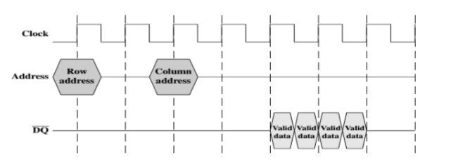
- Traditional DRAM is asynchronous(异步的)
- The processor presents addresses and control levels to the memory, indicating that a set of data at a particular location in memory should be either read from or written into the DRAM(处理器向内存显示地址和控制级别,指示内存中某个特定位置的一组数据应该从DRAM中读取或写入)
- The DRAM performs various internal functions, such as activating the high capacitance of the row and column lines, sensing the data, and routing the data out through the output buffers, and the processor must simply wait through this delay(DRAM执行各种内部功能,例如激活行和列线的高电容、感知数据并通过输出缓冲区将数据路由出去,处理器必须简单地等待这个延迟。)
- After a delay, the DRAM either writes or reads the data(在延迟之后,DRAM既可以写入也可以读入数据)
- 有了同步存取机制,DRAM就可能在系统时钟的控制下输入和输出数据。处理器或其他控制器发出指令和地址信息,他们被DRAM锁存。
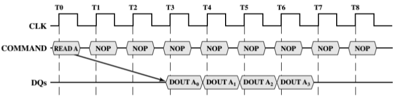
- SDRAM exchanges data with the processor synchronized to an external clock signal and running at the full speed of the processor/memory bus without imposing wait states(SDRAM与外部时钟信号同步并以处理器/内存总线的全速运行的处理器交换数据,而不施加等待状态。)
- Since SDRAM moves data in time with system clock, CPU knows when data will be ready(由于SDRAM随系统时钟及时移动数据,cpu知道数据何时准备好。 )
- 数据读写是在时钟周期的上升点进行
- 异步是需要再次沟通的,而同步是减少一些交互,确定具体的交互时间。(也就是延迟时间)
- 书:111页
3.1.8. DDR DRAM(Double-data-rate SDRAM)
- 在上升的时候可以处理,在下降的时候也是可以进行处理的,在一个存储周期可以读写两次。
- Double-data-rate SDRAM
- Send data twice per clock cycle, once on the rising edge of the clock pulse and once on the falling edge (每个时钟周期传递两次数据,一次在时钟脉冲上升的时候,一次是在时钟脉冲下降的时候)
- Comparison of DDR, DDR2 and DDR3
- Increase operational frequency(增加操作的频率)
- Increase the prefetch buffer(增加提前读取的缓冲)
3.2. Read-only memory(只读存储器)
3.2.1. ROM(只读存储器)
- 必须以掩码的方式写好给我,之后就不能更改了。含有的是不能改变的永久性数据。
- Read-only memory
- Characteristics
- Nonvolatile(非易失性): no power source is required to maintain the bit(不需要提供电来保持数据的位)
- Possible to read a ROM but not possible to write new data(POM可以被读出但是不可以被写入)
- Applications
- Microprogramming, library subroutines, system programs, function tables(微程序设计,库子程序,系统程序,功能表)
- Problems
- Data insertion incurs a relatively large fixed cost(数据插入会产生较大的固定成本)
- No room for error: If one bit is wrong, the whole batch of ROMs must be thrown out(没有容错的空间:一位出错,就必须抛出整批的Error)
- 例子:用于做恢复出厂设置的系统盘,不会有别的危险,因为是不可写的。
- 多用于微编程、系统程序、函数表
3.2.2. PROM(可编程ROM programmed ROM)
- Programmable ROM
- Characteristics
- Nonvolatile(不是易失性的)
- Can be written only once
- Electrically(电写入)
- Special equipment is required for writing(写入需要特殊仪器)
- Compared to ROM
- PROMs provide flexibility and convenience(PROMs提供了灵活性和便利性)
- The ROM remains attractive for high-volume production runs(ROM对于大容量生产运行仍然具有吸引力)
- 例子:写入一些保密程序之类的。
- 为什么用ROM不用PROM:在量产的时候PROM成本高。
3.3. Read-Mostly Memory(主要是进行读操作的存储器)
- Characteristics
- Read operations are far more frequent than write operations(读出的操作比写入操作更加频繁)
- Nonvolatile storage(非易失性存储)
- Types
- EPROM
- EEPROM
- Flash memory
- 为什么不能替代RAM?
- 写起来并不方便(慢)
- 为什么不能替代ROM?
- 他本身是可以修改的,造价比ROM贵。
3.3.1. EPROM(光可擦除/可编程只读存储器)
- Erasable programmable read-only memory
- Characteristics
- Read and written electrically(电写入读出)
- Erasure: exposure of the packaged chip to ultraviolet radiation before a write operation(在写入前,擦除需要专门的紫外线仪器)
- All the storage cells will be the same initial state(所有的存储单元会被处理成相同的状态)
- Take as much as 20 minutes(耗时20min)
- Compared to PROM
- EPROM is more expensive, but it can be updated multiple times(比较贵,但是可以被更新)
- 写入时电写入,擦除使用紫外线照射20min左右,清楚全部数据
3.3.2. EEPROM(电可擦除/可编程只读存储器)
- Electrically erasable programmable read-only memory
- Characteristics
- Can be written into at any time without erasing prior contents(可以在任何时候读入和更新字符,不需要擦除)
- Update the byte or bytes addressed only(仅仅根据数据的地址进行更新)
- Write operation takes several hundred microseconds per byte(写入操作耗时: 几百 ms/byte)
- Compared to EPROM
- EEPROM is more expensive than EPROM and also is less dense(EEPROM比EPROM贵,密度低)。
- 实际上你直接写就行了,而且是字节级来改变。
- 为什么不替代ROM?
- 因为它写起来很慢,操作速度比较慢。
- 比EPROM写入要快
- 集成度比较低
3.3.3. Flash Mmory(快闪存存储器)
- 擦除速度比EPROM快,而比EEPROM慢,并且是一段一段擦除
- 继承度高。
- Characteristics
- Electrically erasing(电擦除)
- Erased in up to a few seconds, much faster than EPROM(可以在几秒内进行擦除)
- Possible to erase on block-level but not byte-level(可以在时钟级别上进行擦除而不是在字节级别上)
- Achieve as high density as EPROM (compared with EEPROM)(达到了和EPROM一样的高密度)
- Compared to EPROM and EEPROM
- Intermediate between EPROM and EEPROM in both cost and functionality(综合价值和功能,在EPROM和EEPROM的中间)
3.4. From Cell to Main Memory(从存储位元到主存储器)
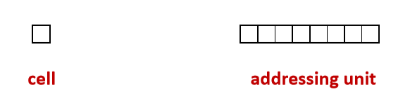
3.4.1. Cell(存储位元)
- 每个寻址单元内的数据不能进行局部修改,都是整体修改。
- Addressable unit
- Composed of the cells with the same address(由有地址的单元格组成)
- Addressing mode
- Byte (common)
- Word
- 现在大多数都是字节可寻址,而之前是字可寻址。
- 而有的天文、数学计算机是有区别的。
3.4.2. 存储阵列
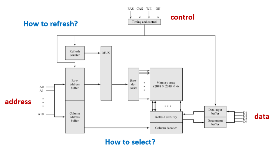
- 为什么是用方形结构?
- 假设一侧有210根线。
- 那么如果是线性的,需要211根线,方形更加节约。
- 选中就是对行和列进行加电,然后同时被加电的地方被选中。
- 能够随机访问的原因?
- 因为我们都是读取地址,然后找到行,找到列,然后选中。所以无论什么单元,都是一样的访问时间。
- 寻址单元

3.4.3. 数据传输率
- 数据传输率 = n/T,其中n是位数,T是存取时间(储存周期)
3.4.4. Refreshing(刷新)
- Centralized refresh(集中刷新)
- Stop read/write operation, and refresh each line(停止一切读写操作,进行刷新)
- The memory cannot be operated when refreshing(在刷新的时候。内存不可以被操作)
- Decentralized refresh(非集中刷新)
- Refresh in each storage cycle when the read/write operation is finished(每一个读写周期(存储周期)刷新一次)
- Increase the time of each storage cycle
- Asynchronous refresh(异步刷新)
- Refresh each line in 64ms(每64ms刷新一次)
- High efficiency (common)(高效的)
- 存在卡顿(按照行或者按照列来充电)问题
- 一般在一个刷新周期中,优先刷新一部分的电
- 如果在一个刷新周期中,有总被使用的,那么我们需要在快到了的时候,停止他,给它充电。
3.4.5. Chips 芯片
- Chip
- Address: A0 – A19
- Data: D0 – D7
- Vcc: power supply
- Vss: ground pin
- CE: chip enable
- Vpp: program voltage
- WE: write enable
- OE: output enable
- RAS: row address select
- CAS: column address select

3.4.6. 内存板 Module organization
- Number of bits extended(位扩展)
- Address line: no change 不变
- Data line: increased 变长
- Use eight 4K1 bit chips to organize 4K8 bit memory
- Length of words extended(字扩展)
- Address line: increased 增加
- Data line: no change 不变
- Use four 16K8 bit chips to organize 64K8 bit memory
- Both extended(位字扩展)
- Address line: increased
- Data line: increased
- Use 8 16K4 bit chips to organize 64K8 bit memory
- 如图,这四块可能最后改装成什么
- 位扩展:有可能变成2000*2000(8 Bits)扩展个数,从同样的位置读出来数据然后拼接成一个更长的数据。
- 数据线会扩展
- 字扩展:还有可能变成1000*1000(32 Bits)扩充位数。
- 我们会对地址线进行扩展
- 因为主要是为了保存成方形的。
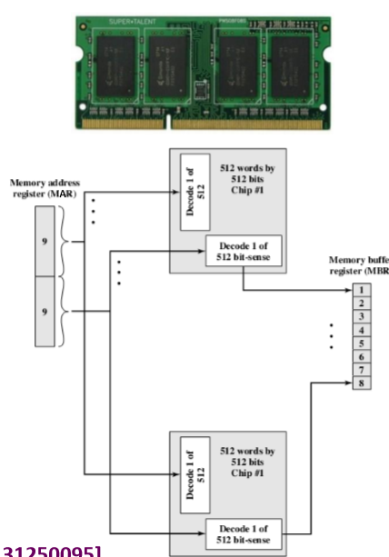
- 位扩展:有可能变成2000*2000(8 Bits)扩展个数,从同样的位置读出来数据然后拼接成一个更长的数据。
3.4.7. Slots(插槽)
- Slots(插槽)
- Combine multiple memory modules(集合多种存储模块)
- Main Memory
- Main memory = RAM + ROM
- Main memory capacity = RAM capacity
- 例子:字扩展:插上两个内存条。
2019-计算机组织与结构-lecture07
https://spricoder.github.io/2020/01/16/2019-COA19/2019-COA19-lecture07/